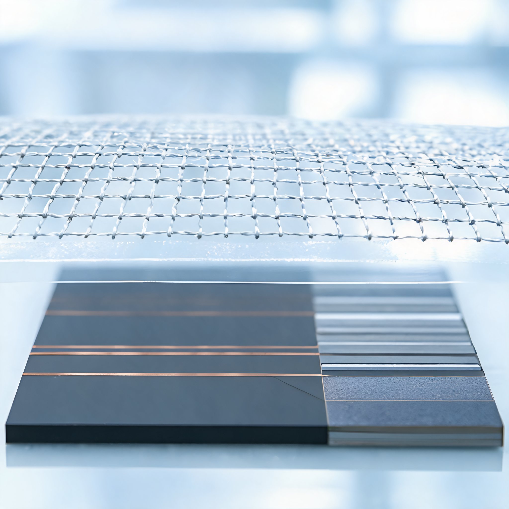
A Chinese research team has identified a wear mechanism that degrades copper-plated silicon heterojunction (HJT) solar cells during screen printing and has proposed a modified screen design to limit the damage. The work focuses on the photoresist-printing step used in copper metallization, where the screen contacts the wafer differently from conventional silver-paste printing.
Screen printing is widely used to form metal contacts on solar cells, but mechanical pressure and thermal treatment can harm sensitive passivating contacts. In HJT cells, that damage can raise recombination losses and lower conversion efficiency. The issue has become more important as manufacturers examine copper plating to reduce silver consumption and metallization cost.
Why photoresist printing is different
Corresponding author Lang Zhou explained that a photoresist screen for HJT cells differs fundamentally from a silver-paste screen. Silver-paste screens have openings covering only 2–5% of the total area, while an emulsion layer covers the rest and keeps the mesh from touching the wafer. Full-area photoresist coating typically uses a screen without emulsion coverage so that resist can be deposited uniformly across the wafer. Consequently, the mesh makes direct and extensive contact with the wafer in every printing cycle.
Earlier investigations cited by the researchers found that conversion efficiency fell from 26.2% to 25.7% over 15,000 consecutive printing cycles in commercial production. Open-circuit voltage and fill factor accounted for most of the loss, while short-circuit current density and electrical resistance remained largely unchanged. Measurements also showed that degradation in minority-carrier lifetime rose from 0.61% with a new screen to 11.0% after 15,000 cycles.
Using three-dimensional confocal microscopy, the team traced the problem to progressive wear of the screen mesh knuckles. As these knuckles wear down, their contact area with the wafer grows, increasing mechanical stress on the passivation layers beneath. Scanning electron microscopy showed no visible surface scratches, but photoluminescence measurements indicated higher recombination losses, pointing to damage at the amorphous silicon/crystalline silicon interface.
Emulsion buffer and trade-off
To prevent direct mesh-to-wafer contact, the researchers added an emulsion buffer layer to the screen. They tested six patterns with emulsion coverage ratios from 2.9% to 16.6%. The results exposed a trade-off: greater emulsion coverage provided more mechanical protection but impaired photoresist distribution.
A coverage ratio of 4.7% gave the best balance. It limited minority-carrier lifetime degradation to 0.41% after 10,000 printing cycles while maintaining relatively good coating uniformity. The team attributed the improvement to the emulsion layer keeping the mesh away from the wafer and thereby reducing cumulative mechanical damage to the passivation layers.
Zhou said the findings show that a relatively simple change to screen design can substantially mitigate printing-induced degradation. The reported result concerns a screen-level modification; the team presented it as a practical approach to improving manufacturing reliability for copper-plated HJT cells.
The study was published in Solar Energy under the title “Screen-printing photoresist induced efficiency degradation and mitigation in Cu-plated SHJ solar cells.” It arrives as copper metallization attracts growing attention as a silver alternative. In April 2026, researchers at China’s Nankai University reported a silver-free HJT cell with 25.2% efficiency using plasma-induced interface engineering and copper electroplating, addressing adhesion, contact resistance and stability at the ITO interface.
Separately, scientists at Germany’s Forschungszentrum Jülich achieved 23.08% efficiency in a fully copper-metallized HJT cell. The silver-free device showed a relatively small efficiency penalty compared with a silver-metallized counterpart, while a cell combining silver-copper paste on the front and silver contacts on the rear reached 23.95%. Those results underline copper’s potential to cut silver use, while indicating that further improvements in processing and electrical performance are still needed.